A Redundant Design for Outdoor Power Battery Management System
The rapid growth of the portable energy storage market has brought about the consumer category of outdoor power supplies, and as consumers' demand for electricity increases, the power of outdoor power supplies continues to increase. In order to ensure the safety of outdoor power sources, the design of a battery management system (BMS) needs to be highly reliable, and some designers may adopt redundant design to achieve this requirement. This article introduces a redundancy design strategy in outdoor power BMS to avoid single point failure.
1. Redundant design of power supply link
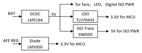
The main electrical devices on the BMS board include MCU, analog front-end, signal conditioning chip, communication chip, etc. Among them, the analog front-end is directly powered by batteries, while signal conditioning, communication, fans, and displays do not directly affect system safety. Instead, the buck chip converts the battery to an appropriate voltage for power supply. The MCU is the most important as it is not only used for receiving, processing, and transmitting data, but also for directly issuing protection commands. Therefore, redundant power supply is required. Common redundant power supply designs are shown in Figure 1.

Figure 1 Outdoor Power BMS Power Supply System Block Diagram
Figure 1 shows that the MCU has two power supply links. The main link is powered by a step-down chip that converts the battery voltage to 3.3V, while the secondary link is powered by an LDO embedded in the analog front-end chip. When the buck chip operates abnormally due to interference or other reasons, causing the MCU to power down and switch to the analog front-end power supply, the system reports an abnormality and stops charging or discharging. In addition, the LDO output of the analog front-end is connected to the MCU for power supply through the Oring module (LM5050), and power is not taken from this link under normal operating conditions. Once the main link loses power, continuously switch to that link for power supply to prevent MCU from powering down and restarting, resulting in data loss. This redundant design can also be used to reduce system power consumption. During normal operation, the system takes power from the buck chip and all peripherals work. After entering the sleep state, the buck chip is disabled, and the MCU is powered by the analog front-end, while other peripherals do not work.
2. Redundant design of sampling link
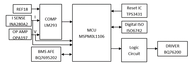
The analog front-end (AFE) chip BQ76952 can be used for monitoring 1-16s battery cells and is suitable for outdoor power supply BMS of 2kw-5kw. AFE comes with battery cell voltage sampling, battery pack voltage sampling, and can also be connected to external sampling resistors to monitor current. To ensure the reliability of the sampling system, external sampling links have been added, as shown in Figure 2, including high-precision current sampling operational amplifier INA280 and universal operational amplifier OPA197 to collect current and battery pack voltage. Under normal operating conditions, there is no significant difference in the voltage and current data obtained by the MCU from the AFE and external sampling link. After average processing, it can be transmitted to the external system. When the data difference between the AFE and external sampling link is too large, the system believes that there is an abnormality and stops charging or discharging externally.

Figure 2 Outdoor Power BMS Functional System Block Diagram
3. Redundant design of reset link
BQ76952 has a Watchdog function, and the feeding time can be configured between 0-65535s. The MCU needs to regularly send instructions to AFE within the dog feeding interval, otherwise it will automatically disable the internal LDO of AFE for a period of time before enabling it, causing the MCU to power down and restart. To ensure the reliability of the reset system, an external reset chip TPS3431 is also used for resetting redundant systems. Under normal operating conditions, the built-in Watchdog of AFE is used to automatically stop charging or discharge externally, while the external chip is used for system reset. During sleep mode, the built-in Watchdog of AFE causes the MCU to power down and restart.
4. Redundant design of protection links
BQ76952 comes with voltage and current protection, and can be configured as multi-level protection. To avoid the system being unable to function when AFE fails, a comparator is added, and the voltage and current obtained from the external sampling link are transmitted to the MCU through the comparator LM293 to obtain a trigger signal. During normal operation, the first two levels of protection are configured in AFE, and the trigger signal obtained by the comparator is used as the third level of protection, as shown in Figure 2.
5. Outdoor power battery pack hot plug design
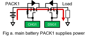
Due to the requirements of many consumers for outdoor power supply range, new design considerations have emerged, which include adding a secondary battery pack to the main battery pack and supporting hot swapping to achieve uninterrupted power supply. However, during the commutation process from the main battery pack to the secondary battery pack, the body diode of the charging FET on the low-voltage side of the battery pack is prone to withstand large currents, leading to overheating, as shown in Figure 3. If the time is too long, it will damage the FET.


Figure 3 Current exchange process from the main battery pack to the secondary battery pack
Due to the system architecture adopting the mode of MCU sending instructions to AFE, as shown in Figure 4, AFE needs to undergo an inherent delay (up to 250ms) to conduct the FET after receiving the conduction command, as shown in Figure 5, which makes the diode withstand long-term high current and easy to damage. Although AFE has body diode protection function, this application scenario cannot enable this function. This is because of the demand for uninterrupted power supply and to prevent the current of the high-voltage battery pack from flowing back into the low-voltage battery pack, the system will first turn off the CHG FET, and the current will be converted to the body diode of the CHG FET. At this point, if the body diode protection function is triggered, the charging FET will automatically conduct again, forming a backflow, so it is not advisable.

Figure 5: There is an inherent delay in the conduction time of AFE
Accelerating the conduction of FETs can reduce the time it takes for the body diode to withstand current. Therefore, during the commutation process, MCU direct drive is used to quickly close the FET to achieve the goal. The control architecture is shown in Figure 6. After combining the DCHG/DDSG signal of AFE with the control signal of MCU and logic, the FET is controlled through high edge drive

Figure 6 Control architecture for adding MCU direct drive
Under normal operating conditions, the MCU is constant to the high level, and the system is controlled by AFE. When hot swapping occurs, the AFE is first constant to the high level, and the MCU signal of the secondary package quickly conducts the switch tube.
- Prev:None
- Next:Shunt voltage regulator alleviates power startup issues
-
Whatsapp

