Shunt voltage regulator alleviates power startup issues
The resistor R forms a low load series connection adjustable bias power supply through RD, parallel voltage regulator IC1, diode D1, and transistor Q1. Select these components to generate the voltage 1 of Q, which falls between the ICs and the turn-off voltage of transmitter 1, as well as the nominal voltage VAUX generated by the output of the rectifier auxiliary bias winding_ NOM. In fact, the V copy pin of voltage 1 on the IC follows wired or in a wired manner, whichever is higher: VAUX_ The transmitter for voltage 1 at NOM or transistor Q.
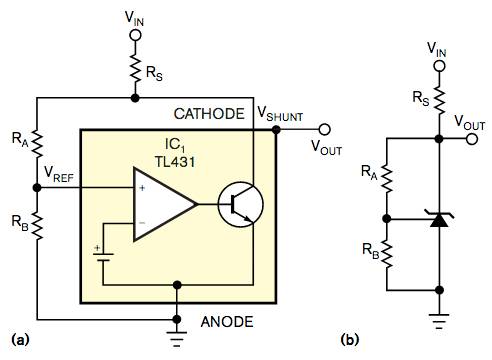
The popular multi terminal TL431 three terminal parallel voltage regulator provides considerable versatility for designers' applications. Figure 1a illustrates the internal circuit of TL431, which includes a precision reference voltage source, an operational amplifier, and a parallel transistor (reference 1). In a typical voltage regulator application, two external resistors R, one and RB, determine the parallel regulated output voltage S at the lower end of the load resistor R (Figure 1b). For example, TL431 and some external active and passive components can be used as low-power auxiliary power supplies for SMPS (switching mode power supply) PWM (pulse width modulation) controllers. In some power supply designs, the auxiliary winding on the step-down transformer supplies power to the PWM controller. Under light output loads, the auxiliary winding may provide insufficient power to the PWM controller.

The simple block diagram (a) in Figure 1 hides the internal complexity of TL431, but you only need three external resistors to connect to the basic parallel regulator circuit (B).
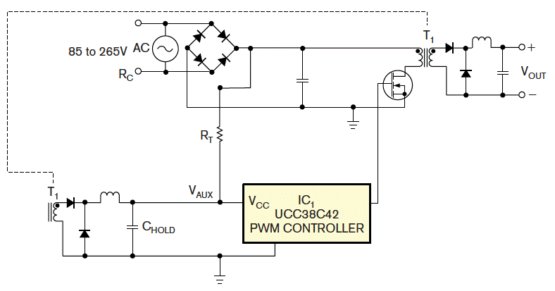
For example, converter circuit diagram 2 shows the PWM controller IC obtaining power. 1. Through auxiliary bias winding and W auxiliary, it is a part of transformer T. 1. The resistor RT and capacitor C form a trickle charging circuit to provide starting power for the IC. 1. To save energy, the resistor R.T provides sufficient current to trickle charge C to voltage V auxiliary. After the circuit starts, it operates as expected and provides output power to the load, The auxiliary winding and its components supply power to the PWM controller.

Figure 2 shows a PWM power supply controller with auxiliary winding as the power source.
However, removing the output load will reduce the energy provided to the auxiliary bias winding, depleting the charge on C and causing IC 1 to shut down, which in turn will disrupt output voltage regulation and lead to irregular power supply operation. The low-power bias power supply circuit provides a light load starting power supply, which is then turned off when the auxiliary winding can provide sufficient energy to the PWM controller IC to save power 1 (Figure 3). In this circuit, the series regulator conducts under light load conditions and turns off when the bias winding can provide energy to the PWM controller, thereby saving energy under load and improving converter efficiency.

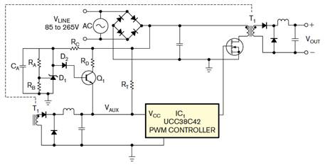
In this improved design, Figure 3, the pulse width controller IC1 derives its RT power supply for startup, auxiliary winding WAUX for normal operation, and parallel voltage regulator circuits IC2 and Q1 for low load operation.
The resistor R forms a low load series connection adjustable bias power supply through RD, parallel voltage regulator IC1, diode D1, and transistor Q1. Select these components to generate the voltage 1 of Q, which falls between the ICs and the turn-off voltage of transmitter 1, as well as the nominal voltage VAUX generated by the output of the rectifier auxiliary bias winding_ NOM. In fact, the V copy pin of voltage 1 on the IC follows wired or in a wired manner, whichever is higher: VAUX_ The transmitter for voltage 1 at NOM or transistor Q. When the auxiliary bias winding and its components provide sufficient power, Q1's transmitter sees reverse bias, and Q1 turns off to save energy. On the contrary, Q1 is lower in power supply assistance than VAUX at V_ NOM has a lighter output load. Note that the circuit must still include a trickle charging resistor R. Due to the integration of undervoltage locking function in most PWM controllers, T can start up above the nominal power supply voltage.
To design a series adjustment regulator, select resistor R. C provides sufficient operating current 2 for the IC, and then selects resistor RD to maintain the collector voltage and current of Q1 within its safe working area. Select resistor R and RB to set the output voltage of the series voltage regulator at the starting voltage of 1 above the IC, which is lower than the nominal voltage provided by the auxiliary winding rectifier output. Select a bypass capacitor C to reduce the ripple voltage on the IC to 2
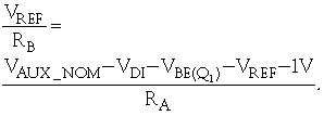
You can use the following equation to adjust the voltage divider formed by resistor R and RB:

The emitter of voltage 1 at Q must be lower than the nominal auxiliary voltage provided by the auxiliary bias winding. The V referee represents a nominal reference voltage of 2.495V inside the parallel regulator IC2, while VD1 and VBE (Q1) represent the voltage drop of D1 and the forward base emitter voltage of Q1.
-
Whatsapp

